AMD and JEDEC Develop DDR5 MRDIMMs With Speeds Up To 17,600 MT/s

MRDIMM
MRDIMM (Image credit: Robert Hormuth/LinkedIn)

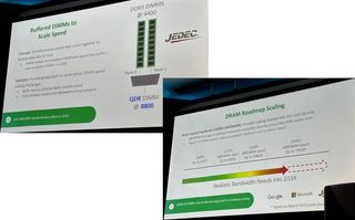
MRDIMMs (multi-ranked buffered DIMMs) could be the standard among buffered DIMMs by 203x. In addition, AMD (opens in new tab) has voiced its commitment at MemCon 2023 to help push JEDEC's MRDIMM open standard, which will significantly boost bandwidth over standard DDR5 DIMMs.

It has been a constant struggle to feed processors with the necessary memory bandwidth as core counts continue to rise. It's one of the reasons why AMD and Intel have shifted over to DDR5 memory on their mainstream processors, such as Ryzen 7000 and Raptor Lake. So you can imagine the challenge in the data center segment with AMD's EPYC Genoa and Intel's Sapphire Rapids Xeon chips pushing up to 96 cores and 60 cores, respectively. 

It gets even more complicated when you slot these multi-core EPYC and Xeon monsters in a 2P or sometimes a 4P configuration. The result is a gargantuan motherboard with an insane number of memory slots. Unfortunately, motherboards can only get so big, and processors keep debuting with more cores. Existing solutions exist, such as unique interfaces like the Compute Express Link (CXL) or High Bandwidth Memory (HBM) formats. MRDIMM aims to be another option for vendors to mitigate the difficulties associated with DRAM speed scaling.

MRDIMM's objective is to double the bandwidth with existing DDR5 DIMMs. The concept is simple: combine two DDR5 DIMMs to deliver twice the data rate to the host. Furthermore, the design permits simultaneous access to both ranks. For example, you combine two DDR5 DIMMs at 4,400 MT/s, but the output results in 8,800 MT/s. According to the presentation, a special data buffer or mux combines the transfers from each rank, effectively converting the two DDRs (double data rate) into a single QDR (quad data rate).

MRDIMM Specifications

Swipe to scroll horizontally
MRDIMMData Rate
Gen18,800 MT/s
Gen212,800 MT/s
Gen317,600 MT/s

First-generation MRDIMMs will offer data transfer rates of up to 8,800 MT/s. After that, JEDEC expects MRDIMMs to improve gradually, hitting 12,800 MT/s and, subsequently, 17,600 MT/s. However, we won't likely see third-generation MRDIMMs until after 2030, so it's a long project.

In conjunction with SK hynix and Renesas, Intel developed Multiplexer Combined Ranks (MCR) DIMMs based on a similar concept to MRDIMM. According to retired engineer chiakokhua (opens in new tab), AMD was preparing a comparable proposition called HBDIMM. Some differences exist; however, no public materials are available to compare MCR DIMM and HBDIMM.

The South Korean DRAM manufacturer expects the first MCR DIMMs to offer transfer rates over 8,000 MT/s, so they are comparable in performance to the first generation of MRDIMM offerings. Intel recently demoed a Granite Rapids Xeon chip with the new MCR DIMMs. The dual-socket system put out a memory bandwidth equivalent to 1.5 TB/s. There were 12 MCR DIMMs clocked at DDR5-8800.

The roadmap for MRDIMMs is vague since it doesn't show when we can expect first-generation MRDIMMs. However, Granite Rapids and competing AMD EPYC Turin (Zen 5) processors will arrive in 2024. Therefore, it's reasonable to expect MCR DIMMs to be available by then since Granite Rapids can use them. Although that hasn't been any official confirmation, it's plausible that Turin could leverage MRDIMMs, given AMD's recent pledge. Therefore, MRDIMMs could potentially arrive in 2024 as well.
Zhiye Liu
RAM Reviewer and News Editor

Zhiye Liu is a Freelance News Writer at Tom’s Hardware US. Although he loves everything that’s hardware, he has a soft spot for CPUs, GPUs, and RAM.

  • jeremyj_83
    This looks like it could be another HBM vs Hybrid Memory Cube situation. It will be interesting to see which memory type becomes the future standard.
    Reply
  • Unolocogringo
    I was thinking DDR vs RDRam fiasco.
    We all know who won that round.
    Reply
  • InvalidError
    jeremyj_83 said:
    This looks like it could be another HBM vs Hybrid Memory Cube situation. It will be interesting to see which memory type becomes the future standard.
    I don't really see this as a competition: on-package and 3D-stacked memory gives you TBs/s bandwidth at the lowest possible latency and power while external memory lets you trade some bandwidth, latency and power for however much memory you want.

    IMO, MRDIMM will be a transient thing: once the cost of on-package memory comes down to the point of becoming the norm and CPUs get enough of it for their intended workloads' typical working set (16-64GB for desktop, 64-256GB for servers), external memory bandwidth and latency won't matter much. Then the external memory controllers will be scrapped in favor of 12-16 extra PCIe lanes per scrapped channel and the option of using CXL-mem for memory expansion instead.

    If JEDEC is going to complexify the DIMM protocol by adding what basically sounds like a multi-channel mux chip on the DIMM, may as well go one step further by offloading basic DRAM housekeeping functions to the mux/buffer chip and turn the CPU-DIMM interface into a simple transactional protocol ("I want to read/write N bytes starting from address X with transaction tag Y and service priority Z"), effectively moving the memory controller off-die.
    Reply
  • hasten
    Unolocogringo said:
    I was thinking DDR vs RDRam fiasco.
    We all know who won that round.
    Rambus? They didnt have to do anything but file lawsuits and settle for royalties from all major dram manufacturers... sounds like a pretty sweat deal!
    Reply
  • hotaru251
    I do wonder to the latency hit compared to normal...also how much more stress does the doubling put on the memory controller?
    Reply
  • InvalidError
    hotaru251 said:
    I do wonder to the latency hit compared to normal...also how much more stress does the doubling put on the memory controller?
    M(C)R-DIMMs don't put any extra load on memory controllers besides the strain from increased bus speed since all control and data signals are buffered on each DIMM and look like a single-point load to the memory controller no matter how many chips are on the buffer's back-end.
    Reply
  • user7007
    So long as on the consumer side we don't have 2 competing standards it sounds good to me. I know intel is showing off similar tech for servers but presumably (hopefully) the JEDEC version is all consumers ever have to worry about. On the server side I'm less worried, intel needs every competitive advantage it can get at the moment.
    Reply
  • lorfa
    Can only read this as "Mister Dimm". Maybe the next standard after that will be "Doctor Dimm".
    Reply
  • bit_user
    I hope this version somehow avoids the tradeoff of doubling the minimum burst length, but I'm not too optimistic.

    hotaru251 said:
    I do wonder to the latency hit compared to normal...
    Well, I think I read MCR DRAM adds a cycle. I'm not sure if that's relative to registered or unbuffered DRAM, though.

    Assuming MR DRAM is implemented the same way, the effect should be similar.
    Reply
  • bit_user
    InvalidError said:
    I don't really see this as a competition: on-package and 3D-stacked memory gives you TBs/s bandwidth at the lowest possible latency and power while external memory lets you trade some bandwidth, latency and power for however much memory you want.
    I think you misunderstood that post. @jeremyj_83 was likening the MCR DRAM vs. MRDRAM contest to that of HMC vs HBM.

    InvalidError said:
    If JEDEC is going to complexify the DIMM protocol by adding what basically sounds like a multi-channel mux chip on the DIMM, may as well go one step further by offloading basic DRAM housekeeping functions to the mux/buffer chip and turn the CPU-DIMM interface into a simple transactional protocol ("I want to read/write N bytes starting from address X with transaction tag Y and service priority Z"), effectively moving the memory controller off-die.
    We don't yet know that they're not, I think?
    Reply