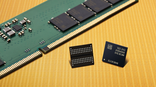
Samsung on Wednesday said (opens in new tab) it had developed its new 16Gb DDR5 memory chips featuring data transfer rates of up to 7200 MT/s. The new ICs will be mass produced next year using the company's latest 12nm DRAM process technology. At present, the company is validating its latest memory devices with AMD.
In addition to being fast, Samsung's 16Gb DDR5 memory chips made using its 12nm node are said to consume up to 23% less power than predecessors (albeit it is unknown at which speed bin) and enable a 20% higher wafer productivity, which essentially means that they are about 20% smaller compared to predecessors and therefore may be cheaper to produce.
The increased bit density and higher default data transfer rates imply that Samsung's 12nm DRAM process technology will enable the company to make higher-density memory ICs as well as devices with higher-than-7200 MT/s speed in the future.

Memory chips rated for an up to 7200 MT/s data transfers at nominal voltage promise to significantly increase performance of next-generation PCs that will be able to take advantage of them. Also, these ICs promise to further push boundaries of DDR5 overclocking for enthusiasts, so we should expect even faster DDR5 modules in 2023 and beyond. Meanwhile, it is noteworthy that right now the company is validating its latest DDR5-7200 chips with AMD, which may imply (although this is a speculation) that the CPU designer plans to support this speed bin rather sooner than later.
"Innovation often requires close collaboration with industry partners to push the bounds of technology," said Joe Macri, Senior VP, Corporate Fellow and Client, Compute and Graphics CTO at AMD. "We are thrilled to once again collaborate with Samsung, particularly on introducing DDR5 memory products that are optimized and validated on 'Zen' platforms."
To get a memory subsystem featuring a 7200 MT/s data transfer rate today, one needs to either use memory modules created for overclockers that usually run at higher-than-nominal voltage or LPDDR5X memory chips. In the former case, the memory subsystem will be power hungry and expensive, whereas in the latter case it will be expensive. Conventional DDR5-7200 memory chips with nominal voltages allow to increase memory bandwidth considerably cheaper.

Samsung's 12nm production node is the company's 5th Generation 10nm-class fabrication process for DRAMs and its 2nd generation technology for memory that uses extreme ultraviolet lithography (EUV). Usage of multiple EUV layers enables Samsung to print circuits faster (i.e., without using multi-patterning) and with greater precision, which may translate into lower costs as well as higher performance and/or power efficiency. In addition to more extensive usage of EUV, Samsung also implemented a new high-k material and refined designs of critical circuits.
Meanwhile, EUV scanners are considerably more expensive than deep ultraviolet (DUV) lithography tools used for memory and logic production, so it is not cast in stone that extensive usage of EUV lowers DRAM production costs at all times, at least for now. Still, we have no idea about Samsung's production costs and therefore will leave this part to DRAM IC analysts.
What is a bit odd is that Samsung does not disclose when exactly it plans to start mass production of its 16Gb DDR5 chips with an up to 7200 MT/s data transfer rate on its 12nm node. 2023 is a rather vague definition as Samsung may start high-volume manufacturing in January 2023, or in December 2023.
The company looks to be somewhat behind its industry peers with its 5th Generation 10nm-class fabrication process. Micron officially started sampling of its LPDDR5X-8500 memory made on its 1β (1-beta) manufacturing technology in early November, though Samsung's usage of EUV might give the company an edge over its rival.

